Demystifying the Miniaturized Marvels: A Guide to Printed Circuit Boards (PCBs)
In today’s tech-driven world, countless electronic devices, from smartphones to spacecraft, rely on a fundamental building block: the Printed Circuit Board (PCB). This seemingly simple board plays a vital role in connecting electronic components and enabling them to function together. But what exactly are PCBs, and how are they made?
This comprehensive guide delves into the fascinating world of PCBs, equipping you with the knowledge to understand their function, composition, and the intricate process of PCB assembly.
The Heart of Electronics: Understanding PCBs
At its core, a PCB is a flat laminate structure that serves two primary purposes:
1- Electrical Interconnection: PCBs provide a conductive pathway for electrical signals to flow between various electronic components. These pathways are created using thin sheets of copper foil etched onto the non-conductive base material.
2- Mechanical Support: PCBs offer a sturdy platform to mount and hold electronic components in place. This ensures proper positioning and stability within the device.
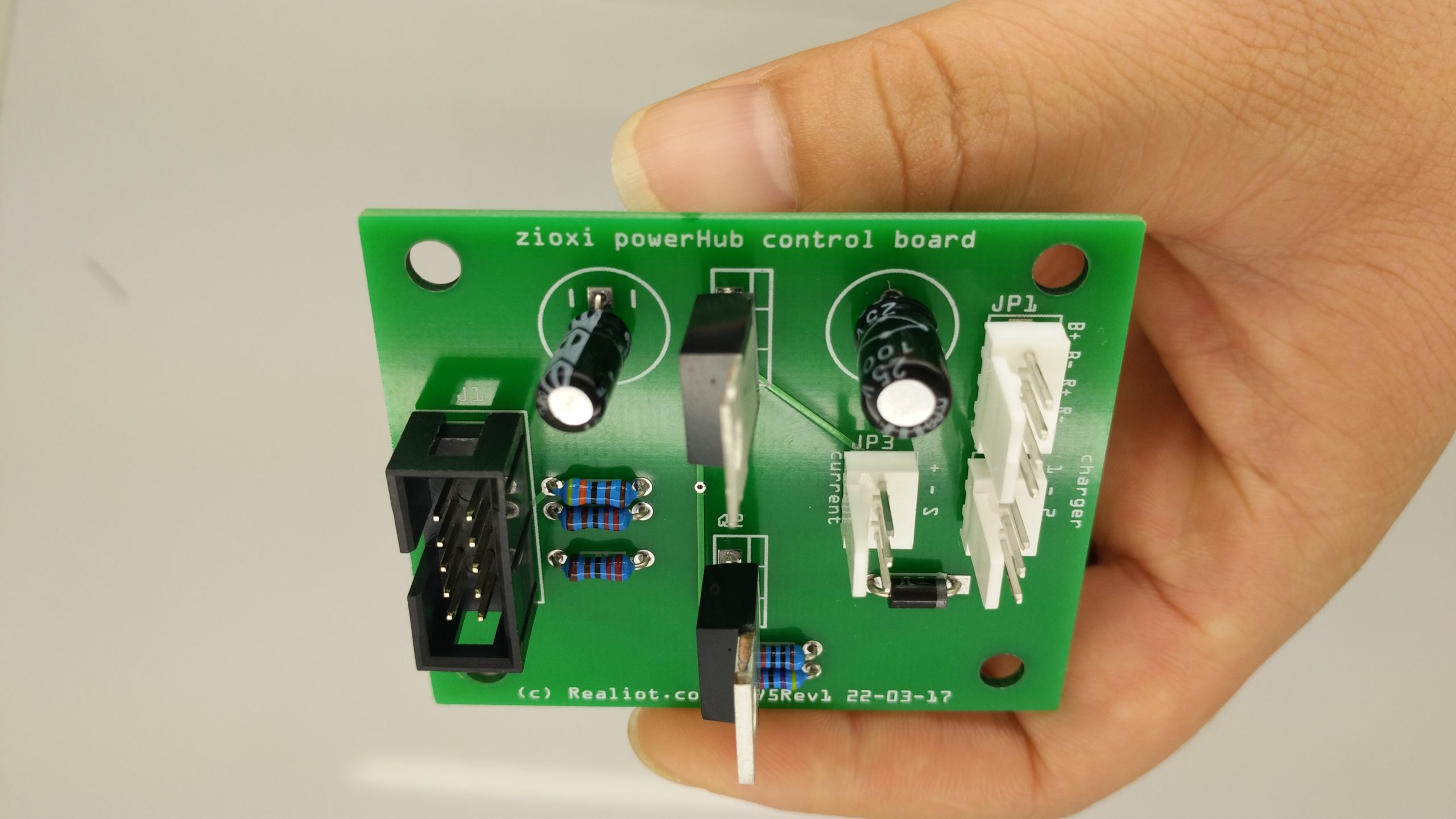
A Layered Masterpiece: The Anatomy of a PCB
While seemingly simple, a NextPCB is a multi-layered masterpiece. The basic structure typically consists of:
Substrate: This forms the foundation of the PCB, usually made from a non-conductive material like FR-4 (flame retardant epoxy laminate) due to its excellent insulating properties.
Copper Foil: Thin sheets of copper are laminated onto the substrate. A chemical etching process removes unwanted copper, leaving behind the desired circuit traces that create the conductive pathways.
Solder Mask: This protective layer covers the PCB, preventing unwanted solder from adhering to unintended areas during PCB assembly. Openings are made in the solder mask to expose the designated soldering pads where components will be attached.
Silkscreen: This top layer acts like a label, displaying essential information like component reference designators and polarity markings. It serves as a visual guide during the assembly process.
Beyond the Basics: Different Types of PCBs
The complexity of a PCB can vary depending on the application. Here’s a glimpse into some common types:
Single-Sided PCB
This is the most basic type, featuring copper traces on only one side of the substrate.
Double-Sided PCB
As the name suggests, this PCB has copper traces on both sides of the substrate, connected by plated through-holes that allow signals to travel between layers.
Multi-Layered PCB
For complex devices requiring high functionality, multi-layered PCBs offer even greater capabilities. These PCBs contain several inner layers of copper traces sandwiched between substrate layers, connected by vias (plated through-holes).
The PCB Journey: From Design to Assembly
The creation of a functional PCB involves a multi-step process:
Design: The PCB layout is meticulously designed using specialized software. This software allows engineers to define the placement of components, routing of circuit traces, and creation of via connections between layers.
Fabrication: The designed PCB layout is sent to a manufacturer who translates the digital file into a physical board. This involves processes like photolithography, etching, and drilling to create the desired circuitry on the substrate.
PCB Assembly: This crucial stage involves mounting electronic components onto the designated pads on the PCB and soldering them securely. This process can be done manually for low-volume production or through automated PCB assembly lines for high-volume manufacturing.
The Intricacy of PCB Assembly: A Look Inside
PCB assembly is a complex and precise operation. Here’s a breakdown of some key steps:
Solder Paste Application: A stencil is used to precisely apply solder paste onto the designated pads on the PCB.
Component Placement: Pick and place machines, or human technicians, carefully position electronic components onto the solder paste deposits.
Soldering: The PCB is exposed to a controlled heat profile, causing the solder paste to melt and permanently attach the components to the pads.
Inspection and Testing: The assembled PCB undergoes rigorous electrical and visual inspections to ensure functionality and identify any potential defects.
The Future of PCBs: Continued Miniaturization and Innovation
The world of PCBs is constantly evolving. As technology demands ever-smaller and more powerful devices, PCB manufacturers are pushing the boundaries of miniaturization. High-density interconnect (HDI) and high-frequency PCBs are just a few examples of advancements in PCB technology.
Conclusion: The Unsung Hero of Electronics
PCBs are the unsung heroes of the electronics revolution. These intricate marvels silently orchestrate the flow of information within countless devices, making modern technology possible.
By understanding the composition, function, and assembly process of PCBs, you gain a deeper appreciation for the engineering marvels that power our daily lives. Whether you’re a hobbyist tinkering with electronics projects or simply someone curious about the inner workings of your smartphone, understanding PCBs unlocks a fascinating world of technological innovation.